Advantages of this solution

High aperture ratio for an extremely light-sensitive imaging system

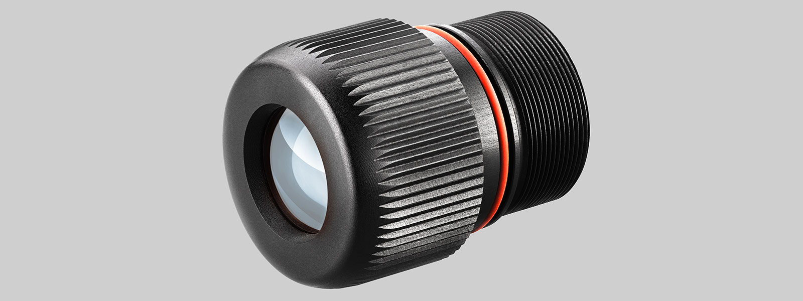
Compact, lightweight design with a total length of just 25.9 mm

Color correction for a spectral range from 400 to 1000 nm

From the idea to the finished solution

Development of the optical concept
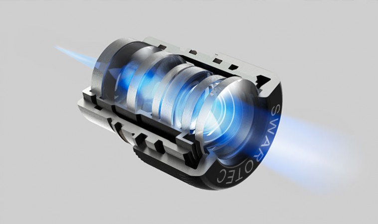
Cutaway model of the objective lens for day/night vision devices

Calculating the optical imaging system required the precise optimization of resolution, modulation transfer function, illumination, and color correction. This needed to be balanced against demanding requirements in terms of dimensions and weight. The optimum compromise was a design comprising 7 lenses, using 4 different types of glass. Finely adjusted error budgets helped achieve an extremely cost-effective implementation.
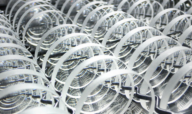
Cutaway model of the objective lens for day/night vision devices
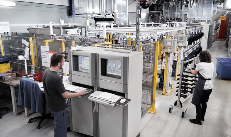
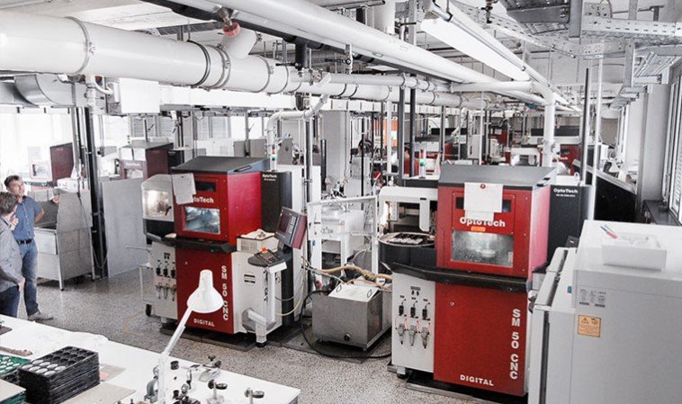
  • Serial production of lenses (up to Ø120 mm)

    Serial production of lenses (up to Ø120 mm)

  • Ultrasonic cleaning of lenses

    Ultrasonic cleaning of lenses

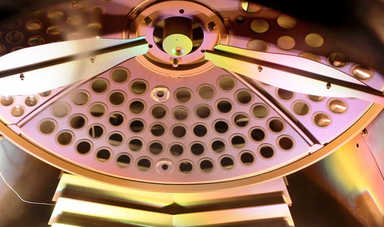
  • Dielectric antireflection coating

    Dielectric antireflection coating

  • Milling of high precision mounts made of magnesium and aluminum

    Milling of high precision mounts made of magnesium and aluminum

  • Turning of shafts and spindles with a precision down to 1 micron

    Turning of shafts and spindles with a precision down to 1 micron

  • Electroplating for scratch-proof anodized surfaces

    Electroplating for scratch-proof anodized surfaces

Challenges of the product

  • Serial production of lenses (up to Ø120 mm)

    Serial production of lenses (up to Ø120 mm)

  • Ultrasonic cleaning of lenses

    Ultrasonic cleaning of lenses

  • Dielectric antireflection coating

    Dielectric antireflection coating

  • Milling of high precision mounts made of magnesium and aluminum

    Milling of high precision mounts made of magnesium and aluminum

  • Turning of shafts and spindles with a precision down to 1 micron

    Turning of shafts and spindles with a precision down to 1 micron

  • Electroplating for scratch-proof anodized surfaces

    Electroplating for scratch-proof anodized surfaces

  • Distortion-free imaging on a CMOS chip with a pixel size of 8.3 µm
  • Small longitudinal chromatic aberration of 0.4 dpt over the entire spectral range
  • High aperture ratio of f/1.2 at an aperture angle of 43°
  • Sales price of EUR 70 with a batch size of 1,000 units

We Are Here to Help You

Just send us an email. We will contact you and answer your questions.

You can also reach us by phone!
Mo. to Th. from 7.30 am to 4.00 pm (CET)
Fr. from 7.30 am to 12 pm (CET)